

The global Probe Card Market represents a vital segment of the semiconductor manufacturing value chain, acting as the physical and electrical interface between an electronic test system and a semiconductor wafer. As microchips become smaller and more complex, the role of the probe card in identifying functional defects early in the production cycle has never been more critical. This specialized equipment allows manufacturers to ensure that only "Known Good Die" (KGD) proceed to the expensive packaging stage, thereby safeguarding profit margins and brand reputation.
Market Overview and Introduction
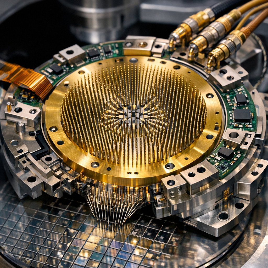
The core of the industry revolves around the precise alignment of microscopic pins or "probes" with the contact pads on a silicon wafer. High-quality semiconductor probe cards are engineered to withstand thousands of touchdowns while maintaining consistent electrical conductivity. As the backbone of wafer testing equipment, these cards have transitioned from simple cantilever structures to sophisticated MEMS-based (Micro-Electro-Mechanical Systems) vertical probes. This evolution is driven by the industry's relentless pursuit of Moore's Law, necessitating testing tools that can handle tighter pitches and higher pin counts.
Key Growth Drivers
The explosive growth of the high-performance computing (HPC) and artificial intelligence (AI) sectors is the primary engine behind the demand for advanced testing solutions. AI chips require massive arrays of interconnects, which in turn demand probe cards with extreme precision. Furthermore, the expansion of the automotive electronics sector, particularly with the rise of electric vehicles (EVs) and autonomous driving systems, has created a need for rigorous testing under various thermal conditions. These industrial shifts ensure a steady demand for high-end testing interfaces that can operate reliably in both cold and hot environments.
Consumer Behavior and E-commerce Influence
While the acquisition of probe cards is a highly technical B2B process, consumer electronics cycles heavily dictate the procurement behavior of semiconductor giants. The seasonal release of smartphones and gaming consoles leads to sudden spikes in orders for specialized IC test probes. Although these items are not purchased via traditional e-commerce, the digital transformation of the supply chain has introduced "e-procurement" portals. These systems allow for real-time tracking of custom designs and facilitate faster communication between the design house and the probe card manufacturer.
Regional Insights and Preferences
Asia-Pacific remains the undisputed leader in this sector, primarily due to the concentration of semiconductor foundries and outsourced semiconductor assembly and test (OSAT) providers in Taiwan, South Korea, and China. In these regions, there is a strong preference for high-parallelism cards that can test dozens of chips simultaneously to maximize throughput. Conversely, the North American and European markets often focus on specialized chip testing solutions for aerospace, defense, and medical applications, where the emphasis is on extreme durability and specialized semiconductor testing tools.
Technological Innovations and Emerging Trends
MEMS technology has revolutionized the industry by allowing for the batch fabrication of probes with near-perfect uniformity. This shift is essential for testing "flip-chip" and "wafer-level packaging" configurations. Another emerging trend is the integration of active components directly onto the probe card to reduce signal noise and improve the speed of data acquisition. Furthermore, as 5G and 6G technologies proliferate, there is an increasing demand for RF (Radio Frequency) probe cards capable of handling ultra-high frequencies without signal degradation.
Sustainability and Eco-friendly Practices
Sustainability in the testing sector is focused on extending the lifecycle of the hardware. Manufacturers are developing modular probe cards where individual probe heads can be replaced or repaired, rather than discarding the entire assembly. This practice significantly reduces electronic waste. Additionally, there is a push to use more environmentally friendly cleaning agents for the probe tips, as traditional chemical solvents are being phased out in favor of mechanical or laser-cleaning technologies that minimize chemical runoff.
Challenges, Competition, and Risks
The primary challenge is the "scaling wall"—as pads on the chips shrink to a few microns, the mechanical stress on the probes increases, leading to faster wear and potential damage to the silicon. Competition is also intensifying as major foundries move toward vertical integration, potentially developing their own internal testing tools. Risks include the high cost of R&D; developing a new probe card architecture requires millions in investment, and a shift in chip design architecture could render a specific probe technology obsolete almost overnight.
Future Outlook and Investment Opportunities
The future of the industry looks bright with the rise of "Chiplets" and 3D heterogeneous integration. These new architectures require testing at multiple stages of the assembly process, multiplying the number of probe cards needed per finished product. Investment opportunities are particularly strong in companies specializing in MEMS vertical probe technology and those developing automated optical inspection (AOI) systems that can verify probe alignment in real-time, reducing downtime for the fab.
Conclusion The evolution of the semiconductor industry relies heavily on the innovations within the testing sector. By providing the precision interfaces needed to validate the next generation of chips, the market remains a cornerstone of modern electronics. As we move toward a more connected and AI-driven world, the demand for sophisticated, durable, and efficient testing solutions will only continue to escalate, offering significant opportunities for those at the forefront of micro-mechanical engineering.
➤➤Explore Market Research Future- Related Ongoing Coverage In Semiconductor Industry: